CALL US
(800) 348-9250

EMAIL US AT
support@pcbunlimited.com
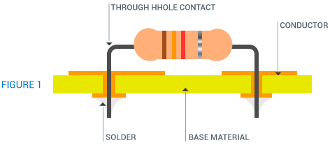
Through-hole technology, also spelled "thru-hole" are holes that go completely through the boards. They can be plated (PTH) or non-plated (NPTH). With plated through holes there is a conductive path from one side of the board to the other, as seen on Figure 1.

This technology was extensively used in PCB Assembly during the 70s and early 80s as a substitute for Point-To-Point constructions. Although the Surface Mount Technology has surpassed the THT as the leading technology for PCB Assembly, THT is still in use nowadays.
Both PTH & NPTH have its own characteristics and uses, and its recommendable to know the differences prior to even start a PCB Design project.
The main characteristic of this type of holes is that, during the manufacturing process, after drilling the boards a thin copper layer is plated onto the walls of the holes, providing them with electrical conductivity. This way, after the PCB Assembly is finished, the link between the component's leads and the copper tracks has a lower resistance and better mechanical stability.
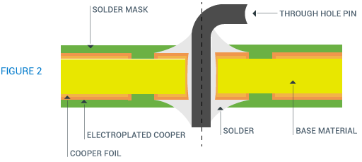
Today most PCBs are double sided, or multi-layered, and most of the Through Holes are plated, this way the components can connect to the required layers in the board. The mounting scheme of a PTH can be seen in Figure 2.

As its name says, in this type of Through Holes there is no copper plated onto the walls of the holes, so the barrel of the hole has not electrical properties. They were very popular when Printed Circuits only had copper tracks printed on one side, but their use decreased as the number of layers in PCBs increased.
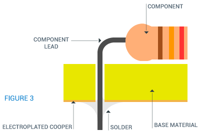
The main advantages of NPTH are that the manufacturing process for these is simpler, and obviously quicker. Nowadays, they are frequently, but not exclusively, used as Tooling/Mounting holes: used to fix the PCB to its operational location. However, they can also be used for components mounting as shown in Figure 3.
