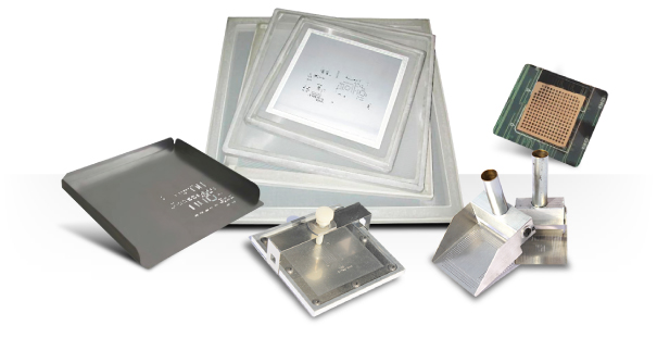
Also known as solder paste stencils or solder stencils, they are usually sheets of stainless steel (or polymer) with apertures. They are designed to deposit solder paste on printed circuit boards but they can also be used to deposit other materials like glue, flux or thermal grease onto a substrate. PCB Unlimited offers a great selection of SMT stencils including rework stencils, electroformed stencils and step stencils:
The stencil thickness and the geometry of the stencil apertures determine the precise volume of solder paste deposited onto the printed circuit boards. The aperture size is also relevant since the relation (aspect ratio) between this and the material thickness will determine if the release of solder paste is optimal. For more information read our article on standard SMT apertures modifications. Controlling these two parameters is crucial to achieve sufficient solder joints. Material thicknesses like 0.004”, 0.005” and 0.006” are the most used for the majority of SMT applications.
Once the solder paste is deposited and the SMT Stencil lifted away from the PCB, the board will be ready for the placement of the SMT components. Read our SMT Stencil step-by-step tutorial
TYPES OF SMT STENCILS:
Laser cut stencils are the most cost effective and the most commonly used in PCB assembly. The new lasers can produce aperture walls that are very smooth. Laser Cutting is a subtractive process where the laser beam completely cuts the aperture out of the metal, one aperture at a time. Electropolish is sometimes used for deburring and nano-coating to improve paste release.
Electroformed stencils are the most expensive, have the longest lead times but have the smoothest aperture walls. Electroforming is an additive process where the stencil is created by electroforming nickel.
Chem-etch stencils are not very commonly used today. They are fabricated using the oldest and least eco-friendly technology. The apertures sidewalls can be rough. Chemical Etching is also a subtractive process where the metal is removed by masking an area with a protectant (photo resist) and then submerging the material into an etchant in order to remove the areas that have not been protected by the photo resist. The stencils created by this process can be of a wide variety of materials.
Our article “Stencils Fabrication Technologies” can be consulted for more information about these processes.


