
CALL US
(800) 348-9250

EMAIL US AT
support@pcbunlimited.com
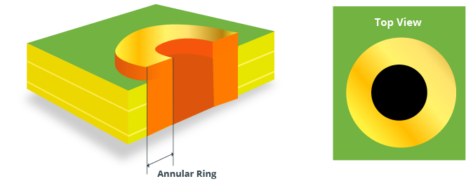
An annular ring is the area of conductive material (usually copper) that surrounds a drilled hole in a PCB. They ensure that there is enough conductive material around the via to maintain a reliable electrical connection even if the hole is slightly off-center due to manufacturing tolerances.
Different types of annular rings correspond to various types of vias and PCB structures. Here are the main types:
These surround holes that go through the entire PCB, connecting all layers from top to bottom. They are common in multilayer PCBs to provide inter-layer connections.
These surround vias that start from an outer layer and connect to one or more inner layers but do not go through the entire printed circuit board. They are used in high-density interconnect (HDI) designs where space on outer layers is limited.
These are around vias that connect only inner layers, invisible from the outer layers. They are used in HDI designs to create internal layer connections without affecting the outer surfaces.
These surround very small vias typically created using laser drilling. They can be blind or buried. They are used for compact, high-density electronic designs.
These are around vias located directly beneath surface mount pads. They are used in high-density designs to save space and improve signal integrity by placing vias directly under components like BGAs.
Consistent Electrical Connections: They ensure a strong and continuous electrical connection between the via and the copper pad. This consistency is very important for maintaining signal integrity across different printed circuit board layers.
Improved conductivity: By providing a large surface area for soldering and plating, annular rings enhance the conductivity and ensure minimal resistance at connection points.
Structural Support: They offer mechanical reinforcement around the vias, helping to resist mechanical stress such as flexing, vibration, and thermal expansion and contraction.
Durability: The structural support translates into greater overall durability for the printed circuit board, making it less susceptible to damage during handling, installation, and operation.
Accommodating Misalignment: During the drilling process, slight misalignments can occur. Annular rings are designed with sufficient width to accommodate these manufacturing tolerances, ensuring the via remains connected to the pad even if the hole is slightly off-center.
Higher Yield: By providing a buffer for drilling inaccuracies, annular rings help improve manufacturing yields, reducing the number of defective boards and associated costs.
Better Solder Joint Formation: The extra copper surface provided by annular rings allows for better solder joint formation, which is critical for both manual and automated soldering processes.
Heat Dissipation: The increased copper area can also provide heat dissipation during soldering, preventing damage to components and improving overall assembly quality.
Multilayer Printed Circuit Boards: Annular rings are crucial in multilayer PCBs, where they facilitate reliable connections between multiple layers, enabling more complex and capable circuitry.
Hight-Density Interconnects (HDI): In HDI printed circuit boards, which feature a higher number of connections per unit area, annular rings enable the use of microvias and other advanced interconnect techniques.
Inspection: Annular rings provide a visual way for quality control inspections, allowing for easier identification of potential issues such as insufficient plating or drilling errors.
Testing: They simplify testing processes, as they provide points for electrical probing and continuity checks.
Minimum Width: Follow industry standards such as IPC-2221, which typically recommend a minimum annular ring width of 0.05 mm (50 microns). Ensure the design software used adheres to these minimum width guidelines to prevent design flaws.
Drill Tolerance: Account for potential misalignments in the drilling process. Design annular rings wide enough to maintain coverage around the via even if the hole is slightly off-center. Add an extra margin to the annular ring width to accommodate these tolerances and prevent potential connection issues.
Copper Thickness: Ensure sufficient copper plating on the annular ring to provide a robust electrical connection and mechanical strength. This is specially important for vias that carry significant current. Aim for uniform copper thickness accorss the printed circuit board to avoid weak points.
Via Aspect Ratio: Maintain a reasonable aspect ratio (via depth to via diameter) to ensure reliable plating and structural integrity. A typical aspect ration guideline is 10:1 or lower. Higher aspect ratios can be more challenging to manufacture and may require advanced techniques.
Surface Finish: Apply suitable surface finishes such as ENIG (Electroless Nickel Immersion Gold) or HASL (Hot Air Solder Leveling) to improve solderability and protect the copper from oxidation. Ensure the finish provides adequate protection against environmental factors that could cause corrotion.
Thermal and Mechanical Stress: Design annular rings to withstand thermal cycling and mechanical stresses. This is critical PCBs to be used in environments with significant temperature fluctuations or physical stresses. Use materials that can handle theses stresses without degrading over time.
Design for Manufacturability (DFM): Ensure that the printed circuit board design is within the manufacturing capabilities of the chosen fabricator. Communicate with manufacturers to understand their limitations and capabilities. Implement process controls to ensure consistency and quality during production.
Component and Assembly Considerations: Ensure that the placement of components does not interfere with the annular rings, especially in dense PCB designs. Solder Mask Clearance: Provide adequate clearance between the annular ring and the solder mask to avoid solder bridging and other assembly issues.
Design Phase: Engineers use computer-aided design (CAD) software to design the PCB layout, including the placement of vias, traces and the size of annular rigns. Designs adhere to industry standards such as IPC-2221, which dictate the minimum annular ring size based on via size and other factors.
Material Selection: The substrate is chosen based on the application requirements. The substrate is clad with a layer of copper, which will be patterned to form the printed circuit board circuitry including annular rings.
Photolithography: A layer of photoresist is applied to the copper-clad substrate. A photomask, which contains the design of the PCB including vias and annular rings, is aligned with the substrate. The photoresist is exposed to ultraviolet light through the mask, hardening the exposed areas.
Etching: The unexposed photoresist is washed away, revealing the copper to be etched. The exposed copper is chemically etched away, leaving the desired copper pattern, including the annular rings.
Drilling: Precision drilling machines create vias at the designated locations. The accuracy of the drilling process is critical to ensure the annular rings remain intact and functional. For PTH vias, the holes are then plated with copper to create electrical connections between different layers.
Plating and Finishing: The entire board is electroplated with copper, increasing the thickness of the annular rings and vias. Additional surface finishes such as ENIG (Electroless Nickel Immersion Gold) or HASL (Hot Air Solder Leveling) may be applied to improve solderability and protect the copper from oxidation.
Inspection and Quality Control:
Inspectors visually check the annular rings and vias for defects such as misalignment, insufficient copper plating, or other issues.
AOI systems scan the printed circuit board to detect any discrepancies in the design specifications. Electrical tests ensure continuity and integrity of the connections, verifying that the annular rings provide reliable electrical pathways.
Solder Mask Application: A solder mask is applied to protect the PCB and prevent solder bridges between traces during component soldering. The solder mask is cured to harden it and provide a durable protective layer.
Legend Printing: Component identifiers and other information are printed onto the PCB using silkscreen printing.
Final Inspection and Testing: A final round of inspections and test ensures the printed circuit board meets all design and quality standards. Functional testing may be performed to verify the performance of the assembled PCB in real-world conditions.