Metal Core PCB (MCPCB) or Insulated Metal Substrate (IMS PCB) is a technology developed to overcome the thermal limitations of the FR4 material. Metal Core is a better choice than FR4 if your boards need to perform in high temperature environment.
Insulated Metal Substrate provides electrical isolation between the copper and the metal core by using a special dielectric with the peculiarity of having high thermal conductivity.
The most common material used in the substrate is aluminum, for this reason, these type of boards are usually known as Aluminum PCBs.
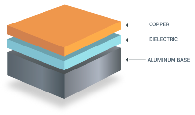
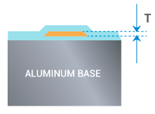
It consists of a single copper conductive layer on top, a
metal base plate (e.g. Aluminum) to provide rigidness to
the circuit board and a thermal conductive dielectric
working as the insulator.
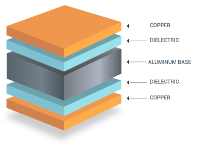
It has two copper layers and the metal core is between the copper layers. Plated Through Holes (PTH) are used tointerconnect the acopper layers so SMT and THT components can be placed on both sides.
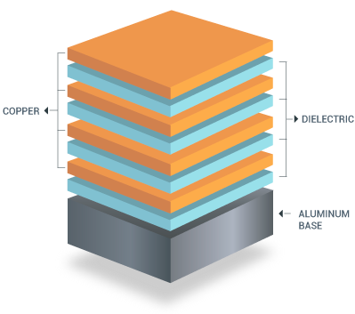
It has more than two conductive layers separated by thermal dielectric. In the bottom of the structure is the metal base. SMT components can only be placed on one side. Not THT components are allowed, but it provides the possibility to make blind and buried vias with internal signal layers and power/ground planes.
| ITEM | DESCRIPTION | SYMBOL | STANDARD | ADVANCED |
| No. of Layer Count | Max Layer Count | NA | 1-4 layer | 1-8 layer |
| T-clad Laminate Supplier | Laminate Supplier | NA | Bergquist, polytronics, boyu | Bergquist, polytronics, boyu |
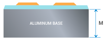
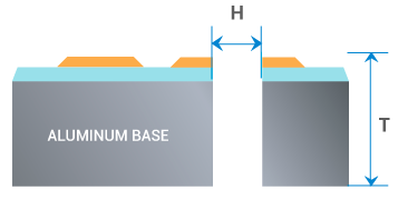
| Metal Thickness | M | 0.4-3.2mm | 0.4-3.2mm | |
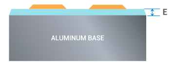
| Dielectric Thickness | E | 100-200um | 100-300um | |
| Thermal Conductivity | NA | 1W/m-k , 2W/m-k 3W/m-k | 1W/m-k , 2W/m-k 3W/m-k , 4W/m-k | |
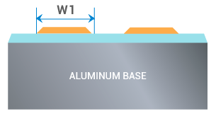
| Circuit Width | Outer Layer Min. Circuit Width | W1 | 0.15mm | 0.15mm |
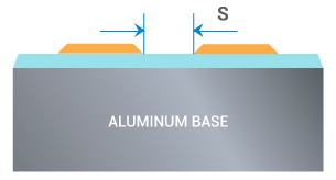
| Circuit Spacing | Outer Layer Min. Circuit Spacing | S | 0.15mm | 0.15mm |
| Copper Foil Thickness | Copper Foil Thickness | T | ½- 4 oz | 1/3 –6 oz |
| Finished Hole | Min. Finished Npth Hole Size | X | 1.0mm | 0.80mm |
| Npth Hole Tol. | A | /-0.05mm | +/-0.05mm | |
| Max. Aspect Ratio | Max. Aspect Ratio | T:H | 8:1 | 10:1 |
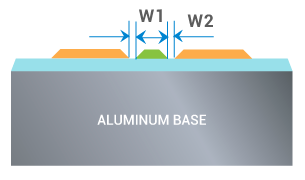
| S/M Dam & Clearance | Min. S/m Dam | W1 | 0.10mm (Green S/M); 0.13mm (white S/M) | 0.10mm (Green S/M); 0.13mm (white S/M) |
| Min. S/m Clearance | W2 | 0.075mm (Green S/M); 0.075mm (white S/M) | 0.05mm (Green S/M); 0.05mm (white S/M) |