Prototype printed circuit boards are what happen when an engineer takes some wire, copper, and plastic components and incorporates them together to create a working device. Circuit boards are found in all aspects of technology, and even though they are popular, each prototype PCB must be assembled differently. So if you are looking to create these magnificent pieces of technology, here are a few things to know about the PCB fabrication process before you start soldering.
The size of the PCB
In simple terms, the size of your circuit board is relative to the overall size of your project. The project size is defined during the electronic engineering process, which is the first thing an engineer must do when they start the project.
How many layers
A PCB layout changes due to the amount of layers it has. Generally, the more layers the PCB has, the more complex the PCB fabrication will be. A breakdown of the amount of layers includes:
Two layered boards: typically these simple PCBs are used in general electronics, such as children toys.
Four layered boards: used for Internet-capable devices, such as a computer. With these boards, the real advantage lays with the fact that its internal layers are usually a dedicated power distribution. This will decrease the loop area and power supply, which will then give a dramatic boost to EMI performance.
Six to eight layers: found in more complex devices, such as smartphones or smart watches.
Information to provide
If you are using a professional service for your PCB fabrication, it is important you provide the company with as much information as you can. This includes the number of layers you are expecting, what material you will be using, the thickness, color, surface finish, copper weight, and gerber file.
Mounting the components
There are two different methods for placing a component on a PCB. They are:
Surface Mount Technology: This is when a machine is able to place components fast and efficiently. It is the most widely used method.
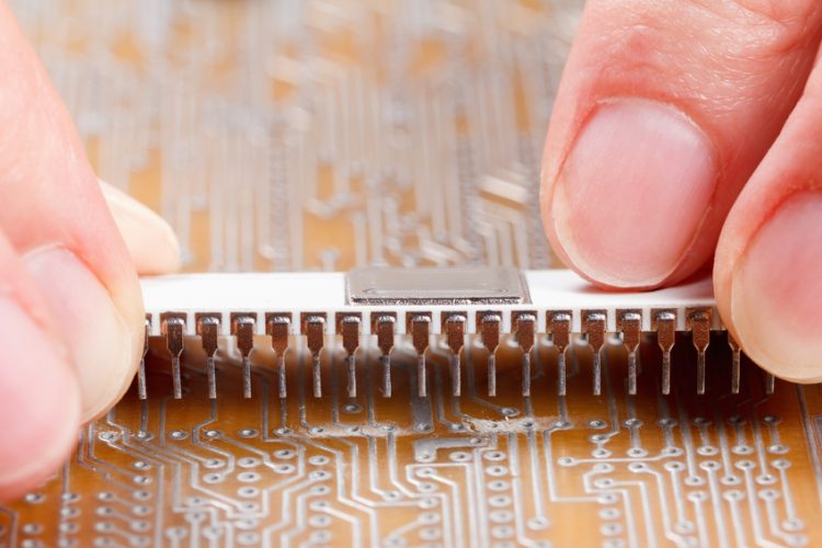
Through-hole: This is when an engineer manually puts components on the PCB through wiring leads into holes in each layer. Generally, this method takes longer and is more expensive.
Have any additional questions about PCB fabrication? Call our experts today.


Short, sweet, to the point, FR-EEexactly as information should be!