
CALL US
(800) 348-9250

EMAIL US AT
support@pcbunlimited.com
A two layer printed circuit board is referred to as double sided board. Circuit boards with more than two layers are multilayer boards. There are many reasons a board design may require more than two layers. Some common reasons for the additional layers are, circuit routing density exceeds two layers, electrical properties, shielding or power distribution. The additional layers are referred to as inner layers. An inner layer is a thin dielectric (0.004” – 0.039”) with a copper pattern etched on each side. A print and etched inner layer is the most common type of inner layer. Inner layers and copper foil are bonded together with prepreg. Prepreg is the basic material from which all epoxy fiberglass circuit boards and laminate are made. Prepreg is fiberglass cloth pre-impregnated with a resin cured to a B Stage. A basic inner layer could have a power or ground on one side and signal traces on the other side. If two inner layers and 2 foil sheets were bonded together this would yield a six layer board. Four signal layers, one power and one ground layer.
All boards designs are created with Computer Aided Design (CAD) stations or simple desktop CAD software. The design is typically the responsibility of the end user and can be designed either internally or by a third party. Once the design is received by the PCB manufacturer the design files are imported into their Computer Aided Manufacturing Software (CAM). The CAM engineer will align the layers in the correct order, perform design rule checks for errors, verify manufacturability, panelize the printed circuit board onto a standard manufacturing panel and then create the production tools. In parallel with CAM, the planning group will review the customer specifications and drawings, check for material availability, create the rout code and the detailed instructions which are required for manufacturing. From this work a Traveler is created which contains the rout code and identifies the process steps and the sequence in which they are to be performed. The Traveler also provides the production floor with detailed instructions and board specifications where they are needed. The Traveler becomes the history of who performed each manufacturing step and when it was completed.
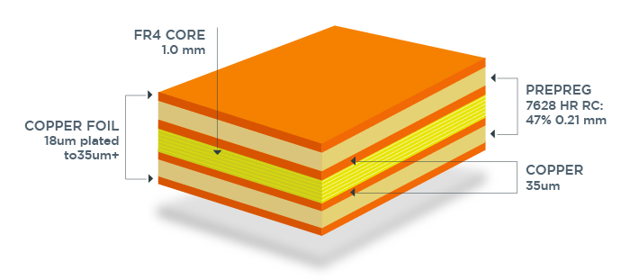
There are various types of laminate materials for the printed circuit board designer to choose from. In most cases the material is specified by the customer. The board material type may be selected based on cost, mechanical properties or the material's electrical characteristics. The most common material is epoxy fiberglass based. Materials are available in a wide selection of base materials, resin systems, a multitude of thicknesses with various copper weights and copper types.
The phototools are one of the production tools created by CAM. Phototools are generated with a laser photoplotter on a sheet of silver halide film. Phototools are used as a mask to transfer the circuit pattern onto the board for subsequent etching, plating or solder mask operations.
Drill files provide the exact hole locations to the drill machines. The drill files also contain the drill parameters for each tool size in the file header. The basic drill parameters are tool diameter, cutting speed, chip load and total allowed hits for each tool. Rout files are very similar to drill files except shapes are being cut instead of holes being drilled. Also, the header information is slightly different due to the type of tools that are used.
Automatic Optical Inspection (AOI) is equipment that uses various light wavelengths or a laser to compare a finished layer to the original CAD data. Each layer that needs to be scanned will have an AOI file. Electrical test files are typically generated from a net list that was provided by the customer with the original CAD data. Test machines at one time used test fixtures that were fabricated for each board design. These designs were typically referred to as bed of nails testing, were costly to fabricate and took considerable time and resources to maintain. One big advantage of this test method was that the test was very fast, just a few minutes depending on the number of test points. Today the trend is towards moving probe testers or flying probe (FP) testers. Flying probe testers are very versatile and require minimal set up time. The main drawback to the flying prob is testing time. Again, depending on the board density the test time could easily be 30 min per panel. Some flying probe testers test boards with a combination of resistive and capacitance measurements to help decrease testing time. In general, the flying probe testers have come a long way since their inception and are very common within the industry.
The first step in building a multilayer printed circuit board is to fabricate the inner layers. The inner layer fabrication process begins with transferring the circuit pattern onto the panel. Circuit patterns are transferred to the panel using a photographic process via photoresist, the photo tool and high intensity light. Photo resist is light sensitive and polymerizes when exposed to light. The first steps in fabricating an inner layer is cleaning the inner layer copper surface and then coating both sides with photoresist aka dry film. Next the photo tool is aligned to the panel and, the image is transferred from the photo tool to the inner layer by exposing the dry film to high intensity light through clear areas of the photo
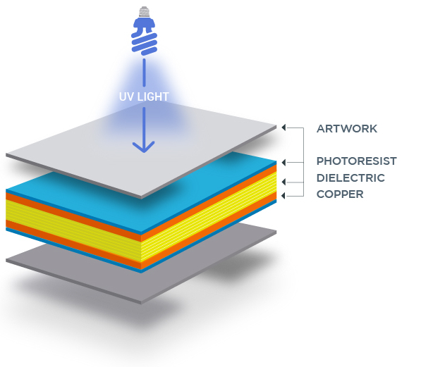
tool. In the case of a print and etch inner layer, the resist which is exposed to the light polymerizes and remains during the dry film developing operation.
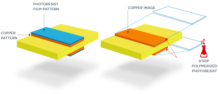
After the inner layer is exposed on both sides it will be processed through a develop/etch/strip line. A DES line is typically a horizontal conveyorized machine approximately 75 feet long. The developer is the first step, the sole purpose of developing is to remove the unpolymerized dry film exposing the base copper. The next step is the etcher which dissolves the unprotected copper. The last step is the stripper which removes the polymerized resist using a high pH solution.
Inner layers are typically inspected by AOI machines. The AOI machine will scan both sides of an inner layer one side at a time, the total process will take several minutes. After scanning each side, the operator can review each of the flagged locations to verify if there is an issue. Once the inner layer has been accepted it is sent to the lamination department.
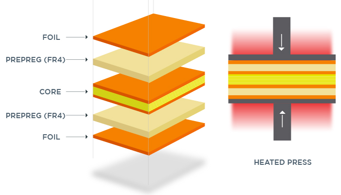
Prior to lamination the inner layers are processed through an oxide process which alters the copper surface topography in order to increase the bond strength of the prepreg to the copper. The layers are assembled into a stack with prepreg used as bonding sheets and then laminated. The lamination process consists of the panels being bonded together in a vacuum at high pressure and high temperature. Each material has its own unique rheology that requires specific lamination parameters. The key parameters are heat rise, cure temperature, cure time and pressure.
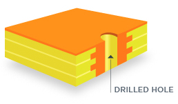
The drilling of the holes is performed on a wide range of CNC machine types. Simpler boards may be drilled with older machine designs that work quite satisfactorily. More complex and denser boards are typically drilled with newer machine designs which have higher rpm spindles, drill extremely fast and are much more accurate. In addition, they may have a tool belt that can hold thousands of tools, a CCD camera for panel alignment and an autoloader and unloader for improved throughput. The panels are drilled for connection to the inner layers, through hole components and mounting holes.
After drilling the holes need to be metallized in order to make electrical connection to the inner layers. The first step in the process is to desmear the holes. The desmear process is designed to remove any resin smear from the drill operation which may electrically insulate the connection to the inner layer or reduce the strength of the plating adhesion to the inner layer. The desmear operation will also, clean the hole of loose debris and add topography to the hole wall for increased adhesion of the initial metallization layer. The second step is to add a thin layer of copper or carbon to the hole wall that will allow for subsequent plating operations.
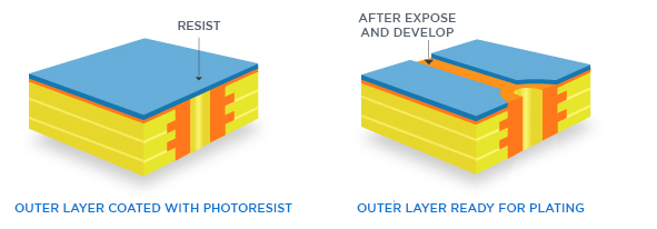
Prior to electroplating the circuit image must be transferred to the outer layers. For the outer layers a reverse outwork is applied. The unwanted areas will be covered by the resist and the designed pattern will be exposed.
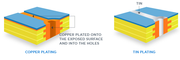
There are various types of plating metallurgies and types of plating options. The most common is pattern plating with a copper plate followed by a tin plate. The copper is required for through hole reliability and current carrying purposes. The tin is required as an etch resist during a subsequent etching operation. Plating of copper in the holes is typically 0.001” followed by a tin plating of 0.0003”. Copper is by far the most common plated metal due to its low cost, easily controlled, and the mechanical/electrical properties are both good.
The panels are then plated with tin, protecting the traces, pads and holes from being etched away when the unwanted copper is removed.
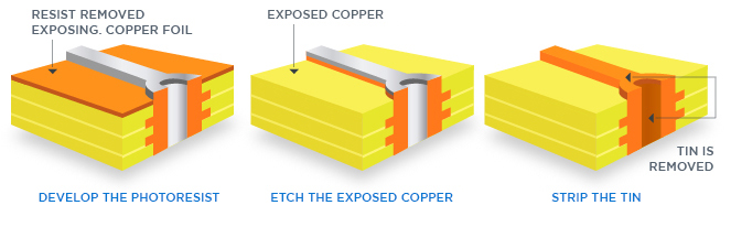
After electroplating the photoresist is stripped from the panel which exposes the background copper for etching. The etching process etches away the exposed copper and the tin protects the copper traces from the top. Some sidewall attack take place on the traces but is compensated for by CAM. After etching the tin is stripped away leaving the copper traces and the plated holes.
Solder mask has several purposes ranging from protecting the traces during assembly operations, defining pads during soldering operations, electrical isolation and protection from the environment. Solder mask and legend inks come in a variety of colors and finishes with green being the most common. Solder mask is typically applied by either screening or spraying. The most common solder masks are photo imageable. After the solder mask is applied to the panel, the process is like dry film photoresists exposing and developing processes.
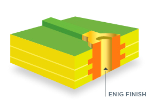
Final finishes are key to the protection of exposed circuitry and the assembly of the components to the printed circuit board. At one time the most common finish was solder. Today there are well over a dozen different finishes, each with their own niche. The change in finishes was brought on by environmental concerns and an increase in circuit densities. Some of the most widely used finishes are Hot Air Solder Leveling (HASL), HASL Lead free, Electroless Nickel Immersion Gold (ENIG), Immersion Tin and Organic coatings.
To get the legend that is often printed on the PCBs and ink-jet
printer silkscreen the board.
This legend usually contains
the component designators, switch settings, and other indications
helpful in assembling, testing and servicing the printed circuit
board.
Printed circuit boards of any complexity are electrical tested to a net list. The net list identifies each circuit on the board. Depending on the overall size of a circuit board, the number of layers and the circuit density, five thousand nets is very common. Once the boards pass electrical test the next step is final inspection. Final inspection is typically a visual inspection looking for cosmetic issues and checking the board to prints to verify the board meets the customers specifications. Final inspection maybe performed at an AQL level or at 100% inspection.
At the final rout operation each board or array is depanelized. In the case of smaller parts that are in an array each piece is almost completely cut out except for some break away tabs. The array helps with handling and assembly of the smaller boards.
Simply give us a call or send us an email. We are here to help.
Phone number: (800) 348-9250
Email: support@pcbunlimited.com